News Story
ISR postdoc helps develop 'nanosponge' that erases and repairs incredibly small errors
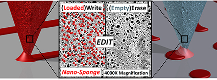
At left, the nanosponge is loaded with particles that are deposited by sliding the sponge along the surface. At right, an empty nanosponge “eraser” that can wet and erase dried up materials. In the center, the real image of the sponge magnified 4000 times with an electron microscope. CREDIT: Nanoscience Exploration Research and Development (NERD) Lab, SIUC.
An ISR postdoctoral researcher is part of a team that has developed a tiny “nanosponge” editing tool that could someday make a big impact in semiconductor, electronics and even biotechnology manufacturing—industries that use lithographic printing techniques in manufacturing.
Pradeep Ramiah Rajasekaran is first author of a new study, “Polymeric lithography editor: Editing lithographic errors with nanoporous polymeric probes,” published in the June 8 issue of the American Association for the Advancement of Science journal, Science Advances. Download the PDF here.
The research was part of Rajasekaran’s graduate work at Southern Illinois University (SIU), where he completed his Ph.D. in Chemistry and Biochemistry under the guidance of Professor Punit Kohli.
Lithography is a centuries-old printing method that takes advantage of the naturally resisting chemical properties of liquids and polymers to force materials like ink into only certain areas of a plate. From the plate the ink is transferred to the material to be printed. Offset printing, a lithographic process, is how most books, magazines and newspapers are made. Since the 1960s, the lithographic process also has been used to mass produce integrated circuits, and more recently, to fabricate micro and nano devices.
At the nanoscale (a nanometer is 1-billionth of a meter), lithography is prone to a variety of errors. Only a handful of techniques are available for correcting them, and all are labor-intensive, expensive and time consuming. Errors are so difficult to correct that industry prefers to discard defective products rather than attempt to fix them. This can result in 20 percent or higher waste of a production run.
“Correcting errors at the nanoscale is very difficult,” Punit Kohli says. Before the nanosponge “there really wasn’t a good way to do it.”
Writing at the nanoscale has been understood for some time. A tiny pointed instrument that works similar to a quill pen is dipped into whatever “ink” is needed and then moved across a substrate to deposit the material.
To make a nanoscale eraser, the researchers had to develop a similarly pointed instrument. The secret was in the material: something soft, porous and spongy, instead of hard and solid, was needed.
Using an electron microscope, the researchers were able to observe the nature and textures of the materials they were creating and testing. Rajasekaran recalls the moment of discovery as he examined newly created erasers made from agarose, a cousin of cellulose.
“When I first glanced at those beautiful conical nanostructures, which were porous, filled with water and flexible, I was extremely excited about the potential,” he says. “I realized that this material looked exactly like a sponge.”
The material can hold any type of liquid and can clean or erase a nanoscale surface by wetting and absorbing molecules into its porous matrix through diffusion—the same way people use wet sponges to clean untidy surfaces. The liquid also acts as a lubricant, allowing the sponge to slide along the surface free of friction while also soaking up byproducts and debris left by the cleaning process. And, just as a painter uses a sponge roller to transfer paint to walls, nanosponges can precisely deposit new molecules at the erased spots.
The nanosponge is used as part of a polymeric lithography editor (PLE). The 500-nanometer, conically shaped, nanoporous hydrogel tip has proven to be efficient, precise and versatile in correcting lithography errors at the submicrometer molecular scale. It can be monitored and manipulated in real time when it is mounted on piezoelectric motors coupled to an optical microscope. Unlike existing techniques that shave, graft or diffuse and evaporate errors, the nanosponge technique combines “real erasing” of deposited patterns with deposition at erased spots.
The animation shows a green fluorescent material loaded nano-sponge sliding along the surface to make patterns (write). The droplet at the tip facilitates the transfer of the materials between the tip and the surface. After writing, a wet nano-sponge (blue) is used to erase the previous pattern. After erasing, new materials (red) is loaded into the nano-sponge and new pattern is re-written on the same area with high precision and accuracy. CREDIT: Dr. Pradeep R. Rajasekaran and Xiaotian Ma, University of Maryland
The versatile nanosponge could open up new and exciting uses for lithography at the micro and nanoscale that previously have remained unexplored because of the error correction issue. It also has the potential to evolve into a 3D etcher similar to 3D printers.
"Dr. Rajasekaran and his collaborators have demonstrated a unique direct writing tool at the nanoscale,” says Institute for Systems Research Director Reza Ghodssi, who currently supervises Rajasekaran’s postdoctoral work. “This technology could have tremendous impact—for example, in the future it could potentially hold very small regents and samples in a clinical setting for high throughput, programmable screening of bio-markers of different diseases.”
"This approach provides a promising route to 'fix' manufacturing errors for micro3D printing applications," says University of Maryland Assistant Professor Ryan Sochol (ME). "In particular, the ability to integrate their nanoporous probe with micro3D printers and/or bioprinters could allow researchers to erase printing mistakes during print runs. Such developments could greatly extend the capabilities of today's micro3D printers."
In addition to Rajasekaran and Kohli, the paper’s co-authors are Chuanhong Zhou and Mallika Dasari from SIU’s Chemistry and Biochemistry Department; and Kay-Obbe Voss (GSI Helmholtzzentrum) and Christina Trautmann (Technische Universität), Darstadt, Germany.
ISR would like to thank Tim Crosby (crosby@siu.edu) and Punit Kohli (pkohli@chem.siu.edu) at Southern Illinois University for this story. You can read the SIU press release here. Please direct questions about this work to them.
Published June 9, 2017
Related Stories
Stories / February 19, 2024
Ingestible Capsule Technology Research on Front Cover of Journal
Stories / December 14, 2023
Gut Health Monitoring Gas Sensors Added to Ingestible Capsule...
Stories / May 21, 2023
New ‘FRRB’ packaging technology may solve an ingestible...
Stories / May 2, 2023
Ghodssi invited speaker at NIMH workshop on sensor technologies...
Stories / March 6, 2023
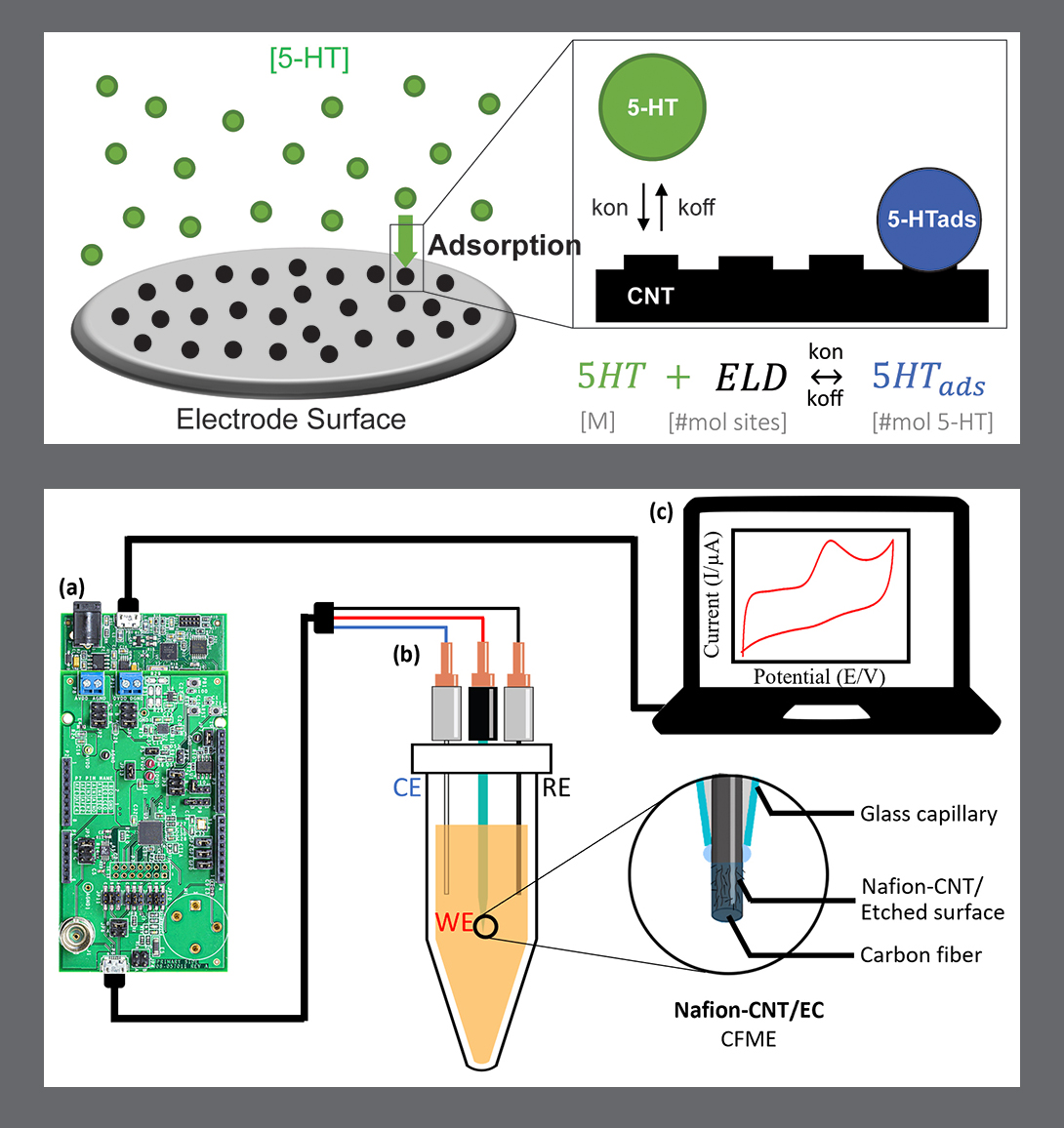
MSAL’s work on serotonin characterization and detection...
Stories / December 5, 2022
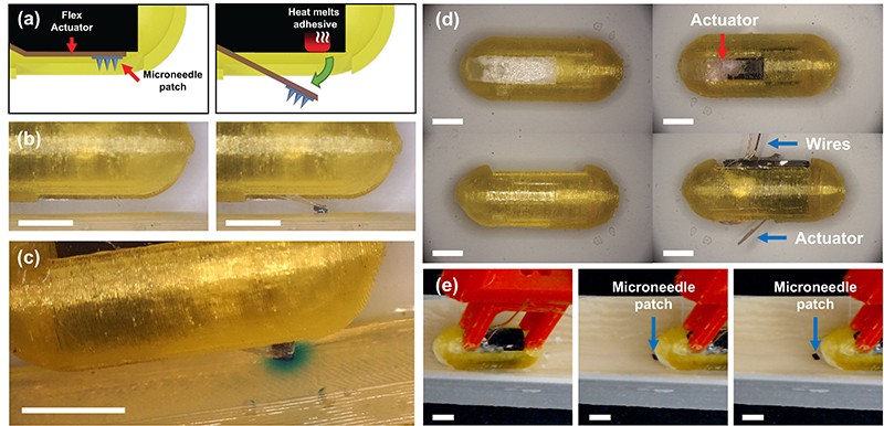
Dropping an anchor for better GI tract disease treatment
Stories / August 10, 2022
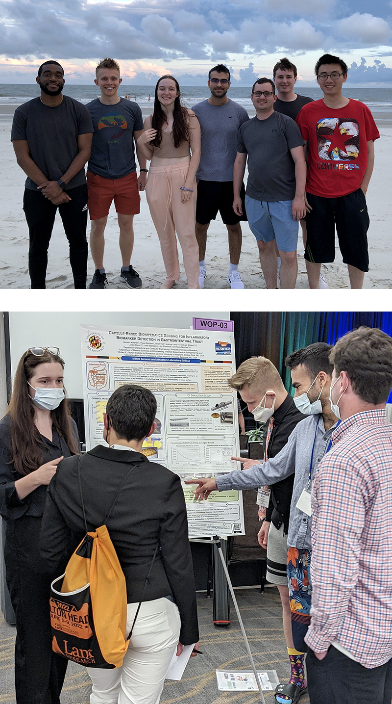
Undergrads and research experiences: Win! Win! Win!
Stories / July 11, 2022
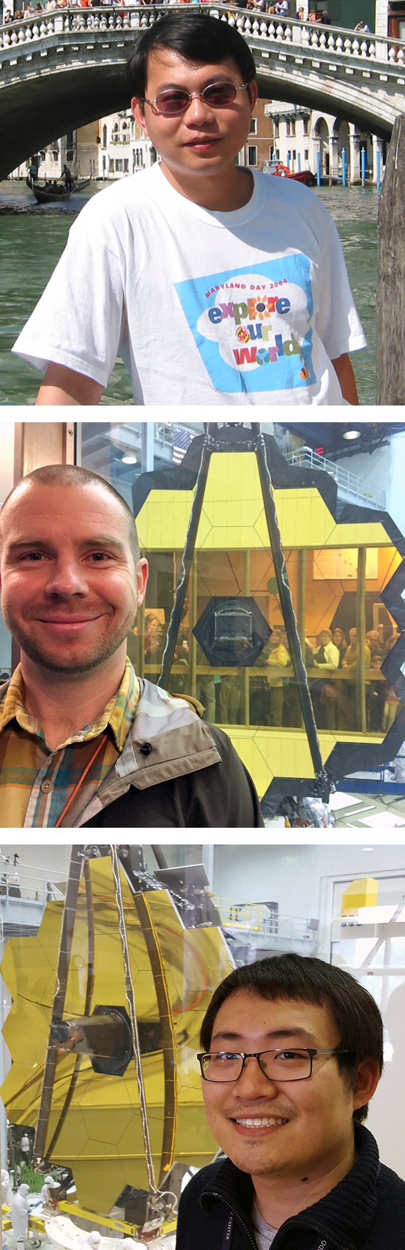
First Webb Space Telescope images are here

Stories / January 2, 2022
UMD engineering alumni contributions aboard James Webb Space...
Stories / September 14, 2021
Fischell Fellowship advances visiting assistant professor’s...